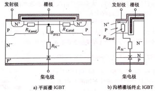
So far, all IGBT designs have a common point planar gate structure. The gate of this shape forms a JFET structure as previously described, as well as a weak conductance modulation effect in the emitter region. For planar gate IGBTs, the concentration of carriers gradually decreases from collector to emitter. The design goal of the new generation IGBT is to maintain a uniform distribution of carrier concentration, preferably gradually increasing, which can further reduce the on-state loss without affecting the tail current and the turn-off loss, resulting in a trench gate structure. appear.
Figure 1a shows the PT based The internal structure and electric field distribution diagram of the trench gate IGBT of the IGBT principle, and FIG. 1b is an enlarged view of the trench gate structure taken by the electron scanning microscope. The main difference between this structure and the conventional planar gate structure is that when the IGBT is turned on, the inversion channel of the P-type emitter region is vertical rather than lateral, which means that there is no JFET effect. Due to the injection of a large amount of electrons, the conductance modulation efficiency near the emitter region is high.

All of this has a positive effect on the concentration of carriers. For comparison, Figure 2 shows a comparison of the carrier concentration inside the trench gate and planar gate structure IGBT. It is quite obvious that from the collector to the emitter, the carrier concentration of the trench gate IGBT is gradually increased, while the planar IGBT is the opposite. The design of the carrier concentration in the emitter region is related to many factors, including the size of the IGBT cells and the distance between them, which makes the adjustment of the carrier concentration infinitely possible. However, it should be borne in mind that a higher carrier concentration is beneficial to reduce the on-state loss; on the other hand, the fewer carriers, the better the reduction of turn-off loss. It has been shown that an internal uniform or slightly increasing carrier concentration facilitates balancing the static and dynamic losses of the trench gate IGBT.

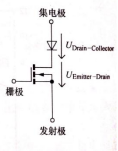
According to the simplified circuit diagram shown in Figure 3, the voltage drop inside the IGBT can be expressed as:
UCEsat=UEmitter-Drain+UDrain-Collector(1)
UEmitter-Drain represents the voltage of the emitter of the IGBT and the drain of the equivalent MOSFET, and UDrain-Collector represents the voltage between the drain and the collector. UEmitter-Drain can be reduced by increasing the width of each IGBT conductive channel. Compared to planar gate IGBTs, the conductive channel of the vertical structure of the trench gate IGBT is more advantageous for designing compact cells. That is, more IGBT cells can be fabricated on the same chip area, thereby increasing the width of the conductive channel. In addition, UEmitter-Drain can be further reduced by eliminating the JFET effect. By adopting these methods, the UEmitter-Drain component in UCEsat can be eliminated. That is to say, for modern IGBTs, the saturation voltage drop is mainly determined by UDrain-Collector.
 ;
;
Increasing the width of the conductive channel facilitates the increase in conductivity, but it also has its disadvantages: a wider conductive channel increases the current when the IGBT is shorted. The most unfavorable situation is that the short-circuit current can be so large that the IGBT is damaged in a very short time. In order for the IGBT to have a short circuit capability of 10 [mu]s (under given test conditions), very careful design of the channel width and adjacent cells is required. To do this, you need to balance the size and spacing of the cells, or do not connect all the gates to the common gate, but directly short the gates and emitters of some cells. The latter is called the insert merge unit process (Plugged Cell Merged, PCM). The planar gate IGBT and trench gate IGBT structure is shown in Figure 4.